
High-Speed Backplane PCB bow causes production failures - an engineering case study
Article written byStuart Sommerville▼
PCB Warpage in a High-Speed Backplane: An Engineering Case Study
PCB warpage is often considered primarily a manufacturing tolerance issue. However, on a large multilayer backplane populated with long surface-mount connectors, even relatively modest bow and twist can become an assembly problem.
During manufacture of a high-speed backplane, we encountered a level of PCB warpage that initially appeared relatively small but was sufficient to interfere with connector placement and soldering.
This case study describes the problem, how it affected assembly, the investigation carried out with the PCB fabricator, and the changes made to the PCB construction and lamination process.
Video: Investigation of PCB warpage and the results following changes to the PCB stack-up and manufacturing process.
The PCB
The design is a large 3.2 mm thick, 8-layer high-speed backplane using a mixed-dielectric construction.
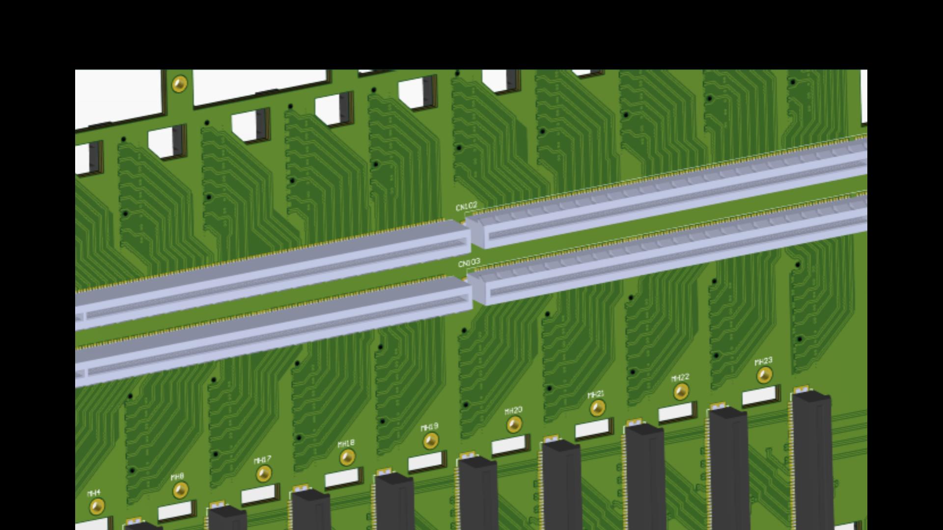
The backplane carries multiple long surface-mount connectors. This is significant because a connector extending over a substantial length of the PCB effectively provides a mechanical reference against which PCB curvature becomes important.
A small amount of PCB bow that might be inconsequential for conventional components can therefore become significant when a long, relatively rigid connector is placed onto the board.
Why was the warpage a problem?
PCB manufacturing standards permit a certain amount of bow and twist, and a PCB does not necessarily need to be perfectly flat to be considered acceptable.
The difficulty in this application was the relationship between PCB flatness and connector length.
The PCIe connectors extend over approximately 50% of the backplane length. Consequently, a relatively small curvature across the PCB can produce a meaningful vertical displacement between the centre and ends of the connector footprint.
During placement, the centre of the connector could contact the PCB while parts of the connector towards its ends remained above the board.
This creates an obvious problem during solder paste reflow: some terminations can sit correctly in the solder paste while others may not achieve the intended contact.
The result can be inconsistent solder joints even though the measured PCB bow or twist might not initially appear severe.
The effect after assembly and reflow
Inspection following assembly demonstrated why PCB warpage mattered in this particular design.
Because the PCB surface was not sufficiently flat relative to the connector body, the connector could not maintain uniform contact with the PCB across its entire length.
Close inspection showed the resulting difference in seating around the connector terminations.
For a high-density backplane, this is undesirable both from a manufacturing-yield perspective and from the standpoint of long-term product reliability.
The issue was therefore referred back to the PCB fabricator for investigation.
Working with the PCB fabricator
The stack-up and manufacturing process were reviewed with the fabricator.
The original construction used RO4350B core material within the mixed-dielectric stack-up. The proposed revised construction changed the relevant high-frequency dielectric arrangement to use prepreg, together with changes to the lamination process.
The fabricator also recommended moving to two press cycles.
An important consequence of the revised construction was a small change in dielectric thickness, which meant that the electrical effect on the controlled-impedance high-speed structures also had to be reviewed before approving the revised stack-up.
This is an important point: a mechanical solution to a PCB problem cannot be considered independently of the electrical design when controlled-impedance high-speed transmission lines are involved.
Why can the lamination process affect PCB warpage?
A multilayer PCB is a composite structure.
Copper, conventional PCB dielectric materials and high-frequency laminates do not have identical thermal and mechanical properties. During lamination they are subjected to elevated temperature and pressure; prepreg resin flows and cures, and the completed structure subsequently cools.
If the resulting stresses are not adequately balanced through the thickness of the PCB, residual stress can remain within the finished board.
On a large PCB, relatively small differences in residual strain through the stack can translate into visible bow or twist.
Changing the dielectric construction and using a staged lamination process gives the fabricator additional control over consolidation of the multilayer structure.
It is important, however, not to attribute the improvement to the number of press cycles alone. In this case both the high-frequency dielectric construction and the manufacturing process were changed.
The appropriate conclusion is therefore that the revised stack-up and lamination process produced a mechanically better result—not that two press cycles will necessarily cure warpage in every PCB design.
The replacement batch
A replacement batch of eight PCBs was manufactured using the revised process.
Each PCB was again checked for bow and twist.
The improvement was immediately apparent.
The replacement boards exhibited very low levels of bow and twist, with only small variations between individual boards.
One board, PCB #8, was judged to exhibit the greatest warpage and was deliberately selected as the first board for assembly.
This effectively provided a worst-case test of the impact on the long surface-mount connectors.
Assembly results
The first replacement PCB assembled successfully.
Inspection after reflow showed:
- the connector end tabs were fully soldered;
- connector pins exhibited good solder fillets;
- pads showed good solder wetting; and
- the assembled board passed inspection and test.
Most importantly, the warpage-related connector seating problem observed previously was no longer apparent.
What did we learn?
There are several useful engineering lessons from this exercise.
PCB acceptance tolerances and assembly requirements are not necessarily the same thing. A board may exhibit an apparently modest amount of bow or twist, but the effect on assembly depends strongly on component geometry.
Long surface-mount connectors are particularly sensitive because they effectively measure PCB curvature over a substantial distance.
Stack-up design has mechanical as well as electrical consequences. In a high-speed PCB we naturally concentrate on impedance, insertion loss, dielectric constant and signal integrity. The mechanical behaviour of the resulting composite structure also needs consideration.
Mixed-dielectric constructions deserve particular attention. Different materials and copper distributions can contribute to an imbalance in the finished laminate.
Manufacturing changes must be evaluated electrically as well as mechanically. Changing core/prepreg construction or dielectric thickness can alter controlled impedance and therefore needs to be reviewed against the electrical design.
Finally, working directly with the PCB fabricator is essential. The fabricator understands the behaviour of their materials and lamination processes in a way that cannot be completely represented by the PCB CAD stack-up alone.
Conclusion
The original production batch demonstrated that relatively modest PCB warpage can have a disproportionate effect when long surface-mount connectors are used on a large high-speed backplane.
Following investigation with the PCB fabricator, the high-frequency dielectric construction and lamination process were revised, including a move to a prepreg-based construction and two press cycles.
The replacement batch demonstrated substantially improved flatness, and the first assembled replacement PCB—selected from the boards showing the greatest residual distortion—assembled and soldered correctly.
The exercise is a useful reminder that successful high-speed PCB design requires consideration not only of signal integrity and electrical performance, but also materials, mechanical behaviour, fabrication and assembly as a complete system.